
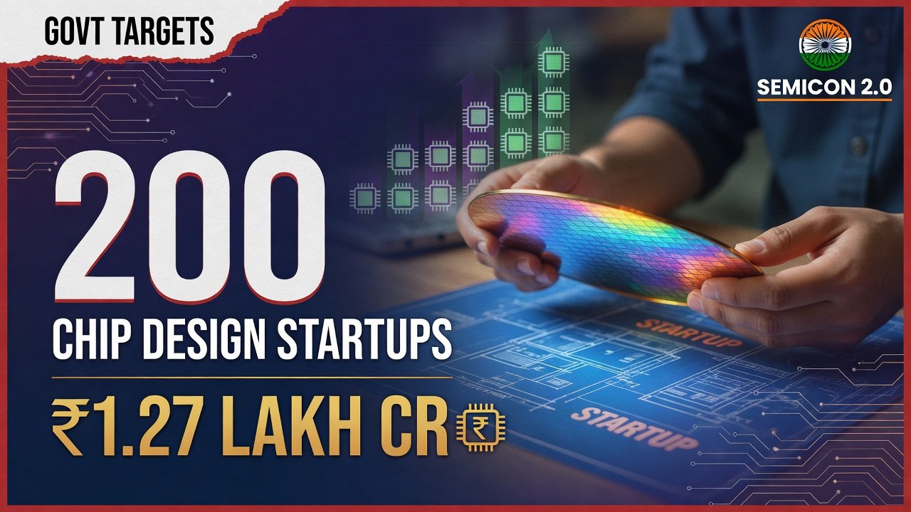
Semicon 2.0 Startup Push: Government Targets 200 Chip Design Startups Under ₹1.27 Lakh Crore Plan
The Semicon 2.0 startup push is placing chip design and semiconductor innovation at the centre of India’s next phase of technology development, with the government targeting at least 200 startups and companies designing chips in India.
Union Electronics and IT Minister Ashwini Vaishnaw announced the target at the inaugural session of SEMICON India 2026 in New Delhi. The initiative is part of the government’s broader Semicon 2.0 programme, which has a total budget outlay of ₹1.275 lakh crore and is designed to strengthen India’s semiconductor ecosystem across design, manufacturing, packaging, equipment, research and talent.
Government Sets 200-Startup Chip Design Target
Under Semicon 2.0, the government intends to support at least 200 startups and companies involved in chip design across different semiconductor requirements.
The target represents a substantial expansion from the first phase of India’s semiconductor programme. More than 105 startups had already started working on chip design under Semicon 1.0, with around 20 securing venture capital funding of approximately ₹800 crore.
The new target therefore focuses on taking India’s chip-design ecosystem beyond its initial stage and creating a larger base of companies capable of developing indigenous semiconductor intellectual property.
₹1.27 Lakh Crore Semicon 2.0 Programme
The Union Cabinet approved Semicon 2.0 in July 2026 with a total financial outlay of ₹1,27,500 crore.
The programme is intended to build on the progress made under the first semiconductor mission and establish long-term policy support for India’s semiconductor design and manufacturing ecosystem.
The government has structured Semicon 2.0 around six major pillars:
- Semiconductor design
- Machines and materials
- Setting up more fabrication units
- Advanced ATMP/OSAT packaging
- Research and development
- Talent development
Together, these areas cover much of the semiconductor value chain, from designing chips to manufacturing, packaging and developing the skilled workforce needed by the industry.
Chip Design Becomes the First Pillar
Chip design has been identified as the first pillar of Semicon 2.0.
The design component covers several categories, including semiconductor intellectual property, chips, system-on-chips and modules for strategic requirements. It also includes commercially focused chip and SoC development and deployment-linked incentives for semiconductor IP and chips.
This approach is particularly relevant to fabless semiconductor startups, which can develop chip architectures and intellectual property without operating their own large-scale fabrication facilities.
India has already built a growing pool of engineers and designers through initiatives supporting electronic design automation tools, training and chip-development programmes.
From 105 Startups to 200 and Beyond
The jump from more than 105 startups attempting chip design under the earlier programme to a target of at least 200 companies represents an effort to broaden India’s semiconductor startup base.
The government has indicated that the previous phase helped establish the foundation, while Semicon 2.0 is intended to scale the ecosystem further.
A larger startup community could potentially create more indigenous semiconductor IP and encourage innovation across areas such as artificial intelligence, automotive electronics, telecommunications, industrial systems, consumer electronics and strategic technologies.
Semiconductor Ecosystem Goes Beyond Chip Manufacturing
The Semicon 2.0 startup push is not limited to encouraging companies to design chips.
The second pillar covers machines and materials, including capital equipment, maintenance facilities, chemicals and gases required by semiconductor manufacturing. Another pillar focuses on additional fabrication facilities, while another strengthens ATMP and OSAT capabilities.
The government is also supporting industry-led research and development and talent development.
This broader structure reflects an attempt to develop multiple layers of the semiconductor supply chain within India rather than concentrating exclusively on chip fabrication.
Government Support for Semiconductor Design
The Semicon 2.0 framework provides fiscal and infrastructure support across the semiconductor value chain.
According to the government’s August notification, the India Semiconductor Mission will act as the nodal agency for the programme. It will invite applications, conduct technical and financial evaluations, recommend applicants and oversee implementation.
Projects supported under Semicon 2.0 will generally have a duration of up to six years, while the scheme is initially open for applications for three years.
The India Semiconductor Mission may also implement design and deployment categories with assistance from C-DAC.
India Builds on Existing Chip Design Momentum
India’s semiconductor ambitions have already produced measurable progress in engineering and chip design.
The government said in August that India had developed 85,000 semiconductor engineers in four years, against an earlier 10-year target. It also said students from Tier-II and Tier-III cities had designed more than 250 semiconductor chips.
These developments provide a talent base for the new startup-focused phase.
The challenge now is to convert engineering capabilities and academic innovation into commercially viable semiconductor companies, intellectual property and products.
Global Investment Is Increasing
The Semicon 2.0 startup push comes alongside growing international interest in India’s semiconductor ecosystem.
At SEMICON India 2026, the government said it had received investment proposals worth approximately $11 billion to $12 billion under the second phase of the semiconductor programme. The proposals span equipment, materials, gases, chemicals and substrates, with investments expected to be realised over the next two to three years, subject to approvals.
Separately, US semiconductor-equipment company Applied Materials announced plans to invest $5 billion in India over the next decade, focusing on areas including research, supply-chain development and workforce expansion.
These developments are occurring alongside India’s efforts to establish domestic fabrication and advanced packaging capabilities.
Why Chip Design Startups Matter
Semiconductor design can provide an important entry point for startups because it does not require every company to own a fabrication plant.
A fabless company can focus on architecture, intellectual property, chip design and system integration while relying on specialised manufacturing partners to fabricate the physical chips.
This model can allow startups to target specialised markets where customised semiconductor solutions are increasingly important.
Areas such as AI accelerators, automotive systems, telecommunications, industrial automation, power management and edge computing could provide potential markets for Indian chip-design companies.
Talent Development Remains a Key Pillar
A semiconductor ecosystem requires more than financial incentives.
Chip architecture, verification, physical design, packaging, manufacturing and equipment engineering all require specialised skills. Semicon 2.0 therefore includes talent development as one of its six pillars.
The government has set an objective of developing 1 lakh technicians and industry-ready professionals as part of the broader semiconductor push.
The combination of startup support and workforce development is intended to create a deeper pool of companies and skilled professionals.
India’s Semiconductor Ambition Expands
The government’s broader semiconductor strategy is also connected to India’s goal of strengthening supply-chain resilience.
Semiconductors are critical components for smartphones, computers, automobiles, telecommunications equipment, industrial machinery, defence systems and artificial intelligence infrastructure.
India’s semiconductor programme has therefore expanded from simply attracting fabrication projects to developing capabilities in design, equipment, materials, packaging, research and talent.
The government’s policy framework aims to create a more complete domestic ecosystem covering these different stages.
Looking Ahead
The Semicon 2.0 startup push marks a significant expansion of India’s semiconductor strategy, with the government targeting at least 200 chip design startups and companies.
The ₹1.27 lakh crore programme combines startup and design support with investments in fabs, advanced packaging, equipment, materials, research and talent.
The key test will be whether the new framework can help Indian companies move from early-stage chip development to commercially successful semiconductor products and intellectual property.
With global semiconductor investment increasing and demand from AI, automobiles, telecommunications and electronics continuing to expand, the coming years will determine how effectively India’s startup ecosystem can translate government support into globally competitive chip-design companies.
FAQs
1. What is the Semicon 2.0 startup push?
It is the semiconductor-focused expansion of India’s industrial policy under Semicon 2.0, including a target of supporting at least 200 chip-design startups and companies.
2. How many chip design startups is India targeting?
The government is targeting at least 200 startups and companies involved in semiconductor chip design.
3. What is the budget of Semicon 2.0?
Semicon 2.0 has a total budget outlay of ₹1,27,500 crore.
4. What are the six pillars of Semicon 2.0?
The six pillars are semiconductor design, machines and materials, fabrication units, ATMP/OSAT packaging, research and development, and talent development.
5. How many startups worked on chip design under Semicon 1.0?
More than 105 startups had started developing chips under the earlier programme, according to the government.
6. What is a fabless semiconductor startup?
A fabless semiconductor company designs chips and develops semiconductor intellectual property but does not necessarily operate its own fabrication plant.
7. Will Semicon 2.0 support semiconductor manufacturing?
Yes. The programme includes support for fabrication facilities, advanced packaging, semiconductor equipment and materials in addition to chip design.
8. How many semiconductor professionals does the government want to train?
The broader Semicon 2.0 plan targets the development of around 1 lakh technicians and industry-ready professionals.
9. Which organisation will implement Semicon 2.0?
The India Semiconductor Mission (ISM) will serve as the nodal agency, handling applications, appraisal, recommendations and implementation oversight.
10. Why is India investing in semiconductor startups?
The initiative is intended to strengthen domestic chip design, intellectual property, manufacturing capabilities and supply-chain resilience while creating a larger base of semiconductor companies and skilled professionals.
- How Effective Leaders Complete More Tasks in Less Time
- Tens of thousands of Zoom users are experiencing outages, which is stopping meetings. What We Know Is Here.
- Peppermint Robotics Raises USD 4 Mn in Series A to Fuel Global Expansion
- Hyderabad Filmmaker Goutham Kool Monkk’s Debut Novel Lieutenant Norman Becomes an Amazon Bestseller on Launch Day

